Showing posts with label electronics. Show all posts

Monday, May 11, 2026

The hidden structure behind a widely used class of materials: Relaxor ferroelectrics

Amazing stuff!

"Materials called relaxor ferroelectrics have been used for decades in technologies like ultrasounds, microphones, and sonar systems. Their unique properties come from their atomic structure, but that structure has stubbornly eluded direct measurement.

Now a team of researchers f... has directly characterized the three-dimensional atomic structure of a relaxor ferroelectric for the first time. The findings ... provide a framework for refining models used to design next-generation computing, energy, and sensing devices. ...

In their paper, the researchers describe how they used an emerging technique to reveal the distribution of electric charges in the material, with a surprising result.

“We realized the chemical disorder we observed in our experiments was not fully considered previously,” ... “Working with our collaborators, we were able to merge the experimental observations with simulations to refine the models and better predict what we see in experiments.” ...

Probing disordered materials

Leading simulations of relaxor ferroelectrics suggest that when an electric field is applied, the interactions of positively and negatively charged atoms in different nanoregions of the material help give rise to exceptional energy storage and sensing capabilities. The details of those nanoregions have been impossible to directly measure to date. ...

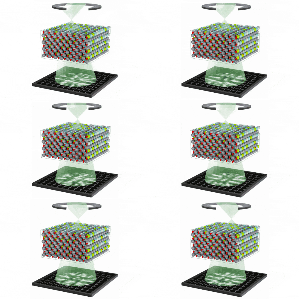
the researchers studied a relaxor ferroelectric material used in sensors, actuators, and defense systems that is a lead magnesium niobate-lead titanate alloy. They used an emerging measurement technique, called multi-slice electron ptychography (MEP), in which researchers move a nanoscale-sized probe of high-energy electrons over a material and measure the resulting electron diffraction patterns. ...

The technique revealed a hierarchy of chemical and polar structures that spanned from atomic to mesoscopic scales. The researchers also found that many regions of differing polarization in the material were much smaller than predicted by the leading simulations. The researchers then fed their new data back into those computer simulations and refined the models to better reflect their findings under different conditions. ..."

From the editor's summary and abstract:
"Editor’s summary
The complexity of lead-based relaxor ferroelectrics makes connecting microscopic characterization with macroscopic properties challenging.
One approach is to compare experimental and theoretical studies, but experiment often averages over material inhomogeneities and theory provides an atomistic view.
To overcome this mismatch, Zhu et al. used multislice electron ptychography, which provided three-dimensional volumetric characterization of the structure and chemistry of a prototypical relaxor material.
Direct comparison with bond valence molecular dynamics simulations revealed that a fully chemically disordered model with residual short-range ordering was necessary to enable agreement with experiment.  ...

Abstract
Introducing structural and/or chemical heterogeneity into otherwise ordered crystals can dramatically alter material properties.
Lead-based relaxor ferroelectrics such as 0.68Pb(Mg1/3Nb2/3)O3-0.32PbTiO3 are prototypical examples.
We performed three-dimensional (3D) volumetric characterization using multislice electron ptychography (MEP) and bond valence molecular dynamics (BVMD) simulations.
Real-space comparisons between the two under varying strain states revealed a coherent 3D view of the “polar slush.” Dipolar correlations from the atomic to domain scales are shown to be jointly modulated by strain and chemical configurations, with the best agreement found in a model accounting for both overall chemical disorder and residual short-range order.
Together, MEP and BVMD provide a framework for linking atomic-scale heterogeneity in complex materials by means of complementary 3D imaging and predictive modeling."

The hidden structure behind a widely used class of materials | MIT News | Massachusetts Institute of Technology "Relaxor ferroelectrics have been used in electronics and sensors for decades, but the source of their unique properties was a mystery until now."


Bridging experiment and theory of relaxor ferroelectrics at the atomic scale with multislice electron ptychography (preprint, open access, published August 2024, could be dated, contains no images)


Using a technique called multi-slice electron ptychography (MEP), researchers move a nanoscale-sized probe of electrons over a material and measure the resulting electron diffraction patterns. Overlapping regions can be used to create a 3-D scan of the material’s atomic structure.


Photonics advance could enable compact, high-performance lidar sensors with no moving parts

Good news!

"... A new study from ... researchers could help to enable next-generation lidar sensors that are compact, durable, and have no moving parts. The key advance is a novel design for a silicon-photonics chip, which is a semiconductor device that manipulates light rather than electricity.  ...

To avoid these drawbacks, the ... researchers designed and demonstrated an array of integrated antennas that minimizes unwanted crosstalk between the antennas. Their innovation allows a lidar chip to scan a wider field of view while maintaining low-noise operation compared to other silicon-photonics-based approaches. ..."

From the abstract:
"Integrated optical phased arrays (OPAs) have emerged as a promising technology for many applications due to their ability to dynamically control free-space optical beams in a compact and non-mechanical manner.
However, these integrated OPAs typically have a restricted field of view (FOV), limited by grating lobes caused by large antenna pitches that are typically necessary to reduce crosstalk between the antennas in the integrated OPA.
In this work, we develop and experimentally demonstrate for the first time, to the best of our knowledge, a set of integrated grating-based antennas with significantly-reduced inter-antenna crosstalk that enable half-wavelength-pitch integrated OPAs with grating-lobe-free and wide-FOV functionality.
First, we derive a generalized theoretical model to describe the coupling dynamics between lossy modes in a system and use this model to analyze the coupling between antennas.
Next, we design and demonstrate a set of three integrated grating-based antennas with different propagation coefficients to enable reduced inter-antenna crosstalk, successfully measuring a significant reduction from 100% to 1% coupling.
Finally, using these reduced-crosstalk antennas, we develop and demonstrate a half-wavelength-pitch integrated OPA, successfully demonstrating grating-lobe-free and wide-FOV functionality.
This work facilitates new functionality for high-performance integrated OPAs."

Photonics advance could enable compact, high-performance lidar sensors | MIT News | Massachusetts Institute of Technology "With a novel design, MIT researchers overcame a stubborn problem that has limited the effectiveness of chip-based systems for lidar."


Fig. 1: Wide-FOV integrated-OPA concept.


Fig. 2: Design of reduced-crosstalk antennas.


Jelena Notaros, senior author (Source)


Tuesday, February 03, 2026

'Thermal diode' design promises to improve heat regulation, prolonging battery life

Good news!

"New technology from University of Houston researchers could improve the way devices manage heat, thanks to a technique that allows heat to flow in only one direction. The innovation is known as thermal rectification ...

These concepts have so far only been demonstrated theoretically, but Zhao aims to build experimental platforms to show the innovation in action. ..."

"Key Takeaways
  • UH researchers developed a way to make heat flow in only one direction, giving engineers new control over how devices manage temperature.
  • The technology works like an electronic diode for heat, helping prevent overheating and potentially extending battery life in phones, electric vehicles and satellites.
  • The approach could lead to cooler, safer and more reliable electronics, especially in extreme environments like space.
...
This new technology gives engineers a new way to control radiative heat with the same precision that electronic diodes control electrical currents, which means longer-lasting batteries for cell phones, electric vehicles and even satellites. It also has the potential to change our approach to AI data centers. ..."

From the abstract:
"As a type of energy carrier, polaritons can play a dominant role in the thermal conductivity of nano/microstructures.
Here, we report an asymmetric thermal conductivity mediated by polaritons that break the Lorentz reciprocity. In contrast to existing approaches that rely on nonlinearity or time modulation, we leverage nonreciprocal polaritons induced by magnetic effects.
We show that nonreciprocal surface plasmon polaritons in time-reversal symmetry-breaking systems, including magneto-optical materials and magnetic Weyl semimetals, can alter the symmetry of thermal conductivity in systems like thin films, resulting in direction-dependent thermal conductivity.
Thermal conductivities of reciprocal material systems can also be made asymmetric through near-field coupling with these material systems. In accompaniment with the surging interest in nonreciprocal thermal radiation by polaritons, we extend the role of nonreciprocal polaritons from radiative heat transfer systems to conduction systems, paving the way for next-generation thermal devices and efficient energy management solutions."


University of Houston Researchers Bring the Heat (original news release) "New Technology Promises to Improve Heat Regulation, Prolonging Battery Life"


Credits: Physiker knacken ein Grundproblem moderner Elektronik

Sunday, October 05, 2025

Major energy savings with new memory chip breakthrough

Good news!

"... Now, researchers have developed layered material that can reduce the energy consumed by memory devices by a factor of 10 by doing away with the need for power-hungry external magnetic fields.

The alloy is made from the magnetic elements cobalt and iron, and nonmagnetic elements germanium and tellurium. It allows 2 opposing magnetic forces to coexist in the same thin material.

Until now, this has only been possible by stacking different ‘ferromagnetic’ and ‘antiferromagnetic’ materials in multilayer structures. ..."

"... To store information, memory devices must switch the direction of electrons within a material. With conventional materials, this typically requires an external magnetic field to alternate the electron orientation. ... new material, however, features a built-in combination of opposing magnetic forces that create an internal force and tilted overall magnetic alignment.

“This tilt allows electrons to switch direction rapidly and easily without the need for any external magnetic fields. By eliminating the need for power-hungry external magnetic fields, power consumption can be reduced by a factor of ten,” ..."

From the abstract:
"The discovery of van der Waals (vdW) magnetic materials exhibiting non-trivial and tunable magnetic interactions can lead to exotic magnetic states that are not readily attainable with conventional materials.
Such vdW magnets can provide a unique platform for studying new magnetic phenomena and realizing magnetization dynamics for energy-efficient and non-volatile spintronic memory and computing technologies.
Here, the coexistence of ferromagnetic and antiferromagnetic orders in vdW magnet (Co0.5Fe0.5)5-xGeTe2 (CFGT) above room temperature, inducing an intrinsic exchange bias and canted perpendicular magnetism is discovered.
Such non-trivial intrinsic magnetic order enables to realize energy-efficient, magnetic field-free, and deterministic spin-orbit torque (SOT) switching of CFGT in heterostructure with Pt.
These experiments, in conjunction with density functional theory and Monte Carlo simulations, demonstrate the coexistence of non-trivial magnetic orders in CFGT, which enables field-free SOT magnetization dynamics in spintronic devices."

Major energy savings with new memory chip breakthrough

Material breakthrough paves way for major energy savings in memory chips (original news release) "It is anticipated that, within just a few decades, the surging volume of digital data will constitute one of the world’s largest energy consumers. Now, researchers ... have made a breakthrough that could shift the paradigm: an atomically thin material that enables two opposing magnetic forces to coexist – dramatically reducing energy consumption in memory devices by a factor of ten. This discovery could pave the way for a new generation of ultra-efficient, reliable memory solutions for AI, mobile technology and advanced data processing."


Figure 1
Coexistence of ferro- and antiferro-magnetic orders in a single atomic stacking nanolayers of (Co0.5Fe0.5)5-xGeTe2. 


Sunday, July 20, 2025

Discovery of a switch in quantum materials could make electronics 1,000 times faster

Amazing stuff!

"... By switching from insulating to conducting and vice versa, the discovery creates the potential to replace silicon components in electronics with exponentially smaller and faster quantum materials.

"Processors work in gigahertz right now," ... "The speed of change that this would enable would allow you to go to terahertz."

Via controlled heating and cooling, a technique they call "thermal quenching," researchers are able to make a quantum material switch between a metal conductive state and an insulating state. These states can be reversed instantly using the same technique. ..."

From the abstract:
"Ultrafast light–matter interaction has emerged as a mechanism to control the macroscopic properties of quantum materials. However, technological applications of photoinduced phases are limited by their ultrashort lifetimes and the low temperatures required for their stabilization.
One such phase is the hidden metallic charge density wave state in 1T-TaS2 [1T phase tantalum disulfide], whose origin and stability above cryogenic temperatures remain the subject of debate. Here, we demonstrate that this phase can be stabilized at thermal equilibrium by accessing a mixed charge density wave order regime through thermal quenching. Using X-ray high-dynamic-range reciprocal space mapping and scanning tunnelling spectroscopy, we reveal the coexistence of commensurate charge density wave and hidden metallic charge density wave domains up to 210 K.
Our findings show that each order parameter breaks basal plane mirror symmetry with different chiral orientations and induces out-of-plane unit cell tripling in the hidden phase. Despite metallic domain walls and a finite density of states, the bulk resistance remains insulating due to charge density wave stacking disorder. Our results establish the hidden state as a thermally stable phase and introduce an alternative mechanism for switchable metallic behaviour in thin flakes of 1T-TaS2 and similar materials with competing phases."

Discovery in quantum materials could make electronics 1,000 times faster


Friday, November 08, 2024

Nanoscale, three-dimensional transistors could enable more efficient electronics

Good news!

"... researchers fabricated a different type of three-dimensional transistor using a unique set of ultrathin semiconductor materials.

Their devices, featuring vertical nanowires only a few nanometers wide, can deliver performance comparable to state-of-the-art silicon transistors while operating efficiently at much lower voltages than conventional devices. ...

The transistors leverage quantum mechanical properties to simultaneously achieve low-voltage operation and high performance within an area of just a few square nanometers. ...

the engineers were able to carefully control the 3D geometry of their transistors, creating vertical nanowire heterostructures with a diameter of only 6 nanometers. They believe these are the smallest 3D transistors reported to date.

Such precise engineering enabled them to achieve a sharp switching slope and high current simultaneously. This is possible because of a phenomenon called quantum confinement.

Quantum confinement occurs when an electron is confined to a space that is so small that it can’t move around. When this happens, the effective mass of the electron and the properties of the material change, enabling stronger tunneling of the electron through a barrier. ...

When the researchers tested their devices, the sharpness of the switching slope was below the fundamental limit that can be achieved with conventional silicon transistors. Their devices also performed about 20 times better than similar tunneling transistors. ...

significantly improving the broken-gap tunnel field effect transistor (TFET) performance. ..."

From the abstract:
"The development of data-centric computing requires new energy-efficient electronics that can overcome the fundamental limitations of conventional silicon transistors. A range of novel transistor concepts have been explored, but an approach that can simultaneously offer high drive current and steep slope switching while delivering the necessary scaling in footprint is still lacking. Here, we report scaled vertical-nanowire heterojunction tunnelling transistors that are based on the broken-band GaSb/InAs system. The devices offer a drive current of 300 µA µm−1 and a sub-60 mV dec−1 switching slope at an operating voltage of 0.3 V. The approach relies on extreme quantum confinement at the tunnelling junction and is based on an interface-pinned energy band alignment at the tunnelling heterojunction under strong quantization."

Nanoscale transistors could enable more efficient electronics | MIT News | Massachusetts Institute of Technology "Researchers are leveraging quantum mechanical properties to overcome the limits of silicon semiconductor technology."

Saturday, September 07, 2024

Controlling molecular electronics with rigid, ladder-like molecules

Amazing stuff!

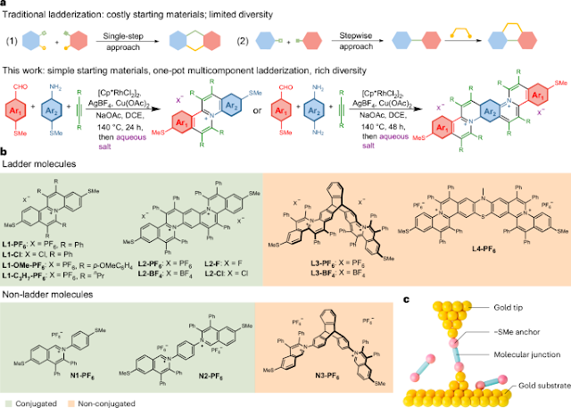
"... University of Illinois Urbana-Champaign researchers report a unique strategy for controlling molecular conductance by using molecules with rigid backbones—such as ladder-type molecules, known as being shape-persistent. Further, they have demonstrated a straightforward “one-pot” method for synthesizing such molecules. The principles were then applied to the synthesis of a butterfly-like molecule, showing the strategy’s generality for controlling molecular conductance.  ..."

From the abstract:
"Molecular electronic devices require precise control over the flow of current in single molecules. However, the electron transport properties of single molecules critically depend on dynamic molecular conformations in nanoscale junctions. Here we report a unique strategy for controlling molecular conductance using shape-persistent molecules. Chemically diverse, charged ladder molecules, synthesized via a one-pot multicomponent ladderization strategy, show a molecular conductance (d[log(G/G0)]/dx ≈ −0.1 nm−1) that is nearly independent of junction displacement, in stark contrast to the nanogap-dependent conductance (d[log(G/G0)]/dx ≈ −7 nm−1) observed for non-ladder analogues. Ladder molecules show an unusually narrow distribution of molecular conductance during dynamic junction displacement, which is attributed to the shape-persistent backbone and restricted rotation of terminal anchor groups. These principles are further extended to a butterfly-like molecule, thereby demonstrating the strategy’s generality for achieving gap-independent conductance. Overall, our work provides important avenues for controlling molecular conductance using shape-persistent molecules."

Controlling molecular electronics with rigid, | EurekAlert!


Wednesday, July 24, 2024

Proton-conducting materials could enable new energy technologies

Amazing stuff! Solid acids!!!

"... Most proton-conducting inorganic materials available now require undesirably high temperatures to achieve sufficiently high conductivity. However, lower-temperature alternatives could enable a variety of technologies, such as more efficient and durable fuel cells to produce clean [???] electricity from hydrogen, electrolyzers to make clean fuels such as hydrogen for transportation, solid-state proton batteries, and even new kinds of computing devices based on iono-electronic effects. ...
In order to advance the development of proton conductors, MIT engineers have identified certain traits of materials that give rise to fast proton conduction. Using those traits quantitatively, the team identified a half-dozen new candidates that show promise as fast proton conductors. ...
proton conduction first involves a proton “hopping from a donor oxygen atom to an acceptor oxygen. And then the environment has to reorganize and take the accepted proton away, so that it can hop to another neighboring acceptor, enabling long-range proton diffusion.” This process happens in many inorganic solids ... Figuring out how that last part works — how the atomic lattice gets reorganized to take the accepted proton away from the original donor atom — was a key part of this research ..."

From the abstract:
"Achieving high proton conductivity in inorganic solids is key for advancing many electrochemical technologies, including low-energy nano-electronics and energy-efficient fuel cells and electrolyzers. A quantitative understanding of the physical traits of a material that regulate proton diffusion is necessary for accelerating the discovery of fast proton conductors. In this work, we have mapped the structural, chemical and dynamic properties of solid acids to the elementary steps of the Grotthuss mechanism of proton diffusion. Our approach combines ab initio molecular dynamics simulations, analysis of phonon spectra and atomic structure calculations. We have identified the donor–hydrogen bond lengths and the acidity of polyanion groups as key descriptors of local proton transfer and the vibrational frequencies of the cation framework as the key descriptor of lattice flexibility. The latter facilitates rotations of polyanion groups and long-range proton migration in solid acid proton conductors. The calculated lattice flexibility also correlates with the experimentally reported superprotonic transition temperatures. Using these descriptors, we have screened the Materials Project database and identified potential solid acid proton conductors with monovalent, divalent and trivalent cations, including Ag+, Sr2+, Ba2+ and Er3+ cations, which go beyond the traditionally considered monovalent alkali cations (Cs+, Rb+, K+, and NH4+) in solid acids."

Proton-conducting materials could enable new green energy technologies | MIT News | Massachusetts Institute of Technology Analysis and materials identified by MIT engineers could lead to more energy-efficient fuel cells, electrolyzers, batteries, or computing devices.


Fig. 1 Steps of proton diffusion via the Grotthuss mechanism in a solid acid.


Tuesday, July 09, 2024

Transistor smaller than a nanometre made with crystal growth

Amazing stuff! Smaller, smaller ...

This research was done at a private university, i.e. Pohang University of Science and Technology.

"A team of Korean researchers has built a transistor smaller than a nanometre.

The researchers have figured out how to grow metallic materials 0.4 nanometres in width, and a few tens of micrometres in length, which they have then incorporated into tiny transistors. ..."

"... To solve this technical problem, the research team leveraged the fact that the mirror twin boundary (MTB) of molybdenum disulfide (MoS₂), a 2D semiconductor, is a 1D metal with a width of only 0.4 nm. They used this as a gate electrode to overcome the limitations of the lithography process. ..."

From the abstract:
"In atomically thin van der Waals materials, grain boundaries—the line defects between adjacent crystal grains with tilted in-plane rotations—are omnipresent. When the tilting angles are arbitrary, the grain boundaries form inhomogeneous sublattices, giving rise to local electronic states that are not controlled. Here we report on epitaxial realizations of deterministic MoS2 mirror twin boundaries (MTBs) at which two adjoining crystals are reflection mirroring by an exactly 60° rotation by position-controlled epitaxy. We showed that these epitaxial MTBs are one-dimensionally metallic to a circuit length scale. By utilizing the ultimate one-dimensional (1D) feature (width ~0.4 nm and length up to a few tens of micrometres), we incorporated the epitaxial MTBs as a 1D gate to build integrated two-dimensional field-effect transistors (FETs). The critical role of the 1D MTB gate was verified to scale the depletion channel length down to 3.9 nm, resulting in a substantially lowered channel off-current at lower gate voltages. With that, in both individual and array FETs, we demonstrated state-of-the-art performances for low-power logics. The 1D epitaxial MTB gates in this work suggest a novel synthetic pathway for the integration of two-dimensional FETs—that are immune to high gate capacitance—towards ultimate scaling."

Transistor smaller than a nanometre made with crystal growth

Scientists Discover Way to “Grow” Sub-Nanometer Sized Transistors (original news release) Opening the Path to Next-Generation Semiconductors through Epitaxial Growth of New Van der Waals Materials


Figure 2. Ultra-miniaturized transistors and integrated circuits using 1D mirror twin boundary gates


Monday, April 03, 2023

A novel ultramicro supercapacitor with ultrahigh charge storage capability

Good news! Note that this research was published by the Indian Institute of Science and the senior author is a woman!

"Researchers at the Department of Instrumentation and Applied Physics (IAP), Indian Institute of Science (IISc), have designed a novel ultramicro supercapacitor, a tiny device capable of storing an enormous amount of electric charge. It is also much smaller and more compact than existing supercapacitors and can potentially be used in many devices ranging from streetlights to consumer electronics, electric cars and medical devices. ...
Supercapacitors, on the other hand, combine the best of both batteries and capacitors – they can store as well as release large amounts of energy, and are therefore highly sought-after for next-generation electronic devices.  ..."

From the abstract (notice the use of the word extraordinary twice):
"On-chip microscopic energy systems have revolutionized device design for miniaturized energy storage systems. Many atomically thin materials have provided a unique opportunity to develop highly efficient small-scale devices. We report an ultramicro-electrochemical capacitor with two-dimensional (2D) molybdenum disulphide (MoS2) and graphene-based electrodes. Due to the tunable density of states, 2D MoS2 provides electric field-induced doping and, combined with a graphene interface, leads to a high carrier mobility. The fabricated solid-state energy storage device is obtained using a gel electrolyte that provides an electrochemical capacitance of 1.8 mF/cm2. An extraordinary enhancement of ∼3000% in electrochemical capacitance (55 mF/cm2from 1.8 mF/cm2, measured from a cyclic voltammetry curve) is observed upon application of back-gate field of −25 V, which is more than the enhancement (18%) observed in a MoS2 electrochemical capacitor (0.95 mF/cm2 from 0.8 mF/cm2) without graphene, whereas the galvanic charge–discharge measurements analysis shows ∼1677% enhancement under the application of −25 V back-gate voltage. Thus, the electric field-induced doping in 2D MoS2, in addition to a high charge carrier mobility due to the graphene, plays a crucial role in an extraordinary large energy storage in the ultramicro-electrochemical capacitor. We also evaluated the capacitance response using an AC signal superimposed with the DC bias to investigate the influence of polarization potential on the electrolyte. The study provides a benchmark development of an ultramicro-electrochemical capacitor for ultrahigh charge storage capability."


Credits: A novel ultramicro supercapacitor with ultrahigh charge storage capability (I am not amused, this article almost copied the entire press release of the Indian Institute of Science without mentioning it or giving due credit)


Schematic of the device


Thursday, March 30, 2023

Researchers create spintronics manufacturing process that could revolutionize the electronics industry

Good news!

"... The new process will allow for faster, more efficient spintronics devices that can be scaled down smaller than ever before. ​​ ...
Spintronic devices, which leverage the spin of electrons rather than the electrical charge to store data, provide a promising and more efficient alternative to traditional transistor-based chips. These materials also have the potential to be non-volatile, meaning they require less power and can store memory and perform computing even after you remove their power source. ...
For the first time, the researchers were able to grow iron palladium on a silicon wafer using an 8-inch wafer-capable multi-chamber ultrahigh vacuum sputtering system, a one-of-a-kind piece of equipment among academic institutions across the country and only available at the University of Minnesota.
“This work is showing for the first time in the world that you can grow this material, which can be scaled down to smaller than five nanometers, on top of a semiconductor industry-compatible substrate, so-called CMOS+X strategies,” ..."

From the abstract:
"As a promising alternative to the mainstream CoFeB/MgO system with interfacial perpendicular magnetic anisotropy (PMA), L10-FePd and its synthetic antiferromagnet (SAF) structure with large crystalline PMA can support spintronic devices with sufficient thermal stability at sub-5 nm sizes. However, the compatibility requirement of preparing L10-FePd thin films on Si/SiO2 wafers is still unmet. In this paper, high-quality L10-FePd and its SAF on Si/SiO2 wafers are prepared by coating the amorphous SiO2 surface with an MgO(001) seed layer. The prepared L10-FePd single layer and SAF stack are highly (001)-textured, showing strong PMA, low damping, and sizeable interlayer exchange coupling, respectively. Systematic characterizations, including advanced X-ray diffraction measurement and atomic resolution-scanning transmission electron microscopy, are conducted to explain the outstanding performance of L10-FePd layers. A fully-epitaxial growth that starts from MgO seed layer, induces the (001) texture of L10-FePd, and extends through the SAF spacer is observed. This study makes the vision of scalable spintronics more practical."


Figure 2
a) Stack structure of the samples with (bottom) and without (top) the MgO seed layer. ...
b) Hysteresis loops ...
c) RAH-Hext loops 


Thursday, March 23, 2023

Single-molecule switch is a million times faster than a transistor

Amazing stuff! Machine learning & AI depend on among other things on better & faster computers!

"... The researchers made a huge breakthrough that could be a game-changer in all tech industries by using fullerene to make a switch from a single molecule. The switching speed is insane, almost a million times faster than a classical computer.
This development could pave the way for the creation of computers beyond what is currently possible with electronic transistors. It could also lead to significant improvements in microscopic imaging, enabling researchers to scrutinize the physical world in unprecedented detail. ..."

From the abstract:
"Single-molecule electron sources of fullerenes driven via constant electric fields, approximately 1 nm in size, produce peculiar emission patterns, such as a cross or a two-leaf pattern. By illuminating the electron sources with femtosecond light pulses, we discovered that largely modulated emission patterns appeared from single molecules. Our simulations revealed that emission patterns, which have been an intractable question for over seven decades, represent single-molecule molecular orbitals. Furthermore, the observed modulations originated from variations of single-molecule molecular orbitals, practically achieving the subnanometric optical modulation of an electron source."

Single-molecule switch is a million times faster than a transistor The ultrafast electron switch could theoretically enable computations orders of magnitude faster than currently possible with classical transistors.

I believe this is the paper:
Light-Induced Subnanometric Modulation of a Single-Molecule Electron Source (open access)

FIG. 1. Conceptual diagram of ultrafast electron emissions from a nano-object by irradiating a light pulse


Schematic representation of a fullerene C60 molecule


Friday, March 10, 2023

Growing Electronics Inside the Brain in live zebra fish and leeches

Amazing stuff! I could use a better brain! 😊 This seems to be early stage research!

"Bioelectronics can be made directly inside the brains of live animals by injecting a cocktail of molecules that can transform into electrically conductive gel, a new study finds.
Swedish scientists have created bioelectronics in live zebra fish and leeches with this new technique. In the long term, the ability to turn any living tissue into electronic matter could make it possible to fabricate microchips in live organisms, the researchers say. ...
The scientists developed a medley of molecules that, when injected into biological tissue, chemically reacted with naturally occurring compounds such as glucose and lactase to form an electrically conducting gel. (Before the injection, the cocktail is not electrically conductive.)
The Swedish researchers first created electronic roses in 2015. However, plant cells possess rigid walls that can serve as scaffolding to help electrodes form, whereas animal cells lack such structures. Creating a mixture of compounds that could form electronics in animals took years of work. ..."

"A recipe for in situ bioelectronic materials
There are challenges in making materials that are soft enough to be interfaced with living tissue but firm enough to be inserted into the body. Strakosas et al. bypassed this challenge by developing a route to the polymer in vivo (see the Perspective by Inal). They introduced a complex precursor system including an oxidase to generate hydrogen peroxide in situ, a peroxidase to catalyze oxidative polymerization, a water-soluble conjugated monomer, a polyelectrolyte with counterions for covalent cross linking, and a surfactant for stabilization. With this cocktail, the authors were able to induce polymerization and subsequent gelation in different tissue environments. Demonstrations include the ex situ fabrication of this conducting gel in zebrafish (brain, fin, and heart), in food samples (beef, pork, chicken, and tofu), and a proof of concept of in vivo stimulation of a leech nerve. ..."

From the abstract of the perspective:
"Electronic devices implanted into a tissue close to neurons of interest are meant to exchange signals with the nervous system. Such bioelectronic devices not only facilitate the study of neural communication, they can also hijack neural circuitry in a therapeutic approach known as bioelectronic medicine. The success of these applications relies on the robustness of the implanted devices and their compatibility with the body. Conventional bioelectronic devices have solid substrates that carry conducting films. Their rigidity can damage soft tissues and reduce an implant’s long-term performance. On page 795 of this issue, Strakosas et al. (1) address the mechanical mismatch between soft and wet biological matter and solid-state electronics and describe an approach that generates electronics directly inside a tissue without a substrate, causing little damage to the tissue."

From the abstract:
"Interfacing electronics with neural tissue is crucial for understanding complex biological functions, but conventional bioelectronics consist of rigid electrodes fundamentally incompatible with living systems. The difference between static solid-state electronics and dynamic biological matter makes seamless integration of the two challenging. To address this incompatibility, we developed a method to dynamically create soft substrate-free conducting materials within the biological environment. We demonstrate in vivo electrode formation in zebrafish and leech models, using endogenous metabolites to trigger enzymatic polymerization of organic precursors within an injectable gel, thereby forming conducting polymer gels with long-range conductivity. This approach can be used to target specific biological substructures and is suitable for nerve stimulation, paving the way for fully integrated, in vivo–fabricated electronics within the nervous system."


Growing Electronics Inside the Brain - IEEE Spectrum Experiments in live zebra fish and leeches may one day lead to growing microchips in living tissue

Perspective Turning tissues into conducting matter An electrically conducting soft polymer is synthesized within living tissue (no public access)

Tuesday, January 24, 2023

Engineers grow “perfect” atom-thin 2D materials on industrial silicon wafers

Good news!

"... Enter 2D materials — delicate, two-dimensional sheets of perfect crystals that are as thin as a single atom. At the scale of nanometers, 2D materials can conduct electrons far more efficiently than silicon. The search for next-generation transistor materials therefore has focused on 2D materials as potential successors to silicon. ...
The team has developed a method that could enable chip manufacturers to fabricate ever-smaller transistors from 2D materials by growing them on existing wafers of silicon and other materials. The new method is a form of “nonepitaxial, single-crystalline growth,” which the team used for the first time to grow pure, defect-free 2D materials onto industrial silicon wafers. ...
With their method, the team fabricated a simple functional transistor from a type of 2D materials called transition-metal dichalcogenides, or TMDs, which are known to conduct electricity better than silicon at nanometer scales. ...
the researchers use conventional vapor deposition methods to pump atoms across a silicon wafer. The atoms eventually settle on the wafer and nucleate, growing into two-dimensional crystal orientations. If left alone, each “nucleus,” or seed of a crystal, would grow in random orientations across the silicon wafer. ... found a way to align each growing crystal to create single-crystalline regions across the entire wafer. ...
To do so, they first covered a silicon wafer in a “mask” — a coating of silicon dioxide that they patterned into tiny pockets, each designed to trap a crystal seed. Across the masked wafer, they then flowed a gas of atoms that settled into each pocket to form a 2D material — in this case, a TMD. The mask’s pockets corralled the atoms and encouraged them to assemble on the silicon wafer in the same, single-crystalline orientation. ... “You have single-crystalline growth everywhere, even if there is no epitaxial relation between the 2D material and silicon wafer.”
With their masking method, the team fabricated a simple TMD transistor and showed that its electrical performance was just as good as a pure flake of the same material.
They also applied the method to engineer a multilayered device. After covering a silicon wafer with a patterned mask, they grew one type of 2D material to fill half of each square, then grew a second type of 2D material over the first layer to fill the rest of the squares. The result was an ultrathin, single-crystalline bilayer structure within each square. ..."

MIT engineers grow “perfect” atom-thin materials on industrial silicon wafers | MIT News | Massachusetts Institute of Technology Their technique could allow chip manufacturers to produce next-generation transistors based on materials other than silicon.


By depositing atoms on a wafer coated in a “mask” (top left), ... can corral the atoms in the mask’s individual pockets (center middle), and encourage the atoms to grow into perfect, 2D, single-crystalline layers (bottom right).


Neuromorphic Memristors Run AI Tasks at 1/800th Power

Good news! Very impressive results! Brains made of silicon!

"... Now two new studies may help solve key problems these components face not just with yields and reliability, but with finding applications beyond neural nets. ...
Such brain-inspired neuromorphic hardware may also prove ideal for implementing neural networks—AI systems increasingly finding use in applications such as analyzing medical scans and empowering autonomous vehicles. ...
researchers in Israel and China fabricated memristive devices using a standard CMOS production line. The resulting silicon synapses the team built boasted a 100 percent yield with 170- to 350-fold greater energy efficiency than a high-performance Nvidia Tesla V100 graphics processing unit when it came to multiply-accumulate operations, the most basic operation in neural networks. ...
The scientists developed the new devices using the floating-gate transistor technology used in commercial flash memory. Whereas conventional floating-gate transistors have three terminals, the new components have only two. ...
The new devices displayed high endurance, operating past more than 100,000 cycles of programming and erasing by using voltage pulses. In addition, they showed only moderate device-to-device variation and are projected to possess long data retention times of more than 10 years. ...
In another study, a team of French researchers investigated using memristors for the statistical computing technique known as Bayesian reasoning, in which prior knowledge helps compute the chances that an uncertain choice might be correct. Its results are fully explainable—unlike many nearly inscrutable AI computations—and it can perform well when there is little available data, as it can incorporate prior expert knowledge. ...
The scientists rewrote Bayesian equations so a memristor array could perform statistical analyses that harnesses randomness—a.k.a. “stochastic computing.” Using this approach, the array generated streams of semi-random bits at each tick of the clock. These bits were often zeroes but were sometimes ones. The proportion of zeroes to ones encoded the probabilities needed for the statistical calculations the array performed. This digital strategy uses relatively simple circuitry compared to nonstochastic methods, all of which reduces the system’s size and energy demands.
The researchers fabricated a prototype circuit incorporating 2,048 hafnium oxide memristors on top of 30,080 CMOS transistors on the same chip. In experiments, they had the new circuit recognize a person’s handwritten signature from signals beamed from a device worn on the wrist. ..."

From the abstract (1):
"Memristors, and other emerging memory technologies, can be used to create energy-efficient implementations of neural networks. However, for certain edge applications (in which there is access to limited amounts of data and where explainable decisions are required), neural networks may not provide an acceptable form of intelligence. Bayesian reasoning could resolve these concerns, but it is computationally expensive and—unlike neural networks—does not naturally translate to memristor-based architectures. Here we report a memristor-based Bayesian machine. The architecture of the machine is obtained by writing Bayes’ law in a way that makes its implementation natural by the principles of distributed memory and stochastic computing, allowing the circuit to function solely using local memory and minimal data movement. We fabricate a prototype circuit that incorporates 2,048 memristors and 30,080 transistors using a hybrid complementary metal–oxide–semiconductor/memristor process. We show that a scaled-up design of the machine is more energy efficient in a practical gesture recognition task than a standard implementation of Bayesian inference on a microcontroller unit. Our Bayesian machine also offers instant on/off operation and is resilient to single-event upsets."

From the abstract (2):
"Memristor-based neuromorphic computing could overcome the limitations of traditional von Neumann computing architectures—in which data are shuffled between separate memory and processing units—and improve the performance of deep neural networks. However, this will require accurate synaptic-like device performance, and memristors typically suffer from poor yield and a limited number of reliable conductance states. Here we report floating-gate memristive synaptic devices that are fabricated in a commercial complementary metal–oxide–semiconductor process. These silicon synapses offer analogue tunability, high endurance, long retention time, predictable cycling degradation, moderate device-to-device variation and high yield. They also provide two orders of magnitude higher energy efficiency for multiply–accumulate operations than graphics processing units. We use two 12 × 8 arrays of memristive devices for the in situ training of a 19 × 8 memristive restricted Boltzmann machine for pattern recognition via a gradient descent algorithm based on contrastive divergence. We then create a memristive deep belief neural network consisting of three memristive restricted Boltzmann machines. We test this system using the modified National Institute of Standards and Technology dataset, demonstrating a recognition accuracy of up to 97.05%."

Memristors Run AI Tasks at 1/800th Power - IEEE Spectrum These brain-mimicking devices boast tiny energy budgets and hardened circuits

(1) A memristor-based Bayesian machine (no public access, but article above contains a link to the PDF file)


Monday, August 22, 2022

Superlattices Could Make Bulky Capacitors Obsolete

Good news!

"... One roadblock to shrinking present-day electronics is the relatively large size of their capacitors. Now scientists have developed new “superlattices” that might help build capacitors as small as one-hundredth the size of conventional ones. ...
 Antiferroelectric materials could help solve this problem. Like magnets, which possess north and south poles, electric charges within materials become separated into positive and negative poles. Antiferroelectrics are materials in which these “electric dipoles” are generally oriented in opposing directions, leading to an overall zero electric polarization. However, when antiferroelectrics are exposed to a strong enough electric field, they can switch to a highly polarized state, resulting in large energy densities. ...
However, relatively few natural antiferroelectric materials are known. In a new study, Aramberri and his colleagues sought to engineer artificial structures that could act like antiferroelectrics. ...
The team then constructed superlattices made of ferroelectric lead titanate (PbTiO3) and paraelectric strontium titanate (SrTiO3). These superlattices got their name because the lead titanate and strontium titanate, themselves arrayed in lattice structures, are also placed in thin, alternating layers with each other. ..."

From the abstract:
"The polarization response of antiferroelectrics to electric fields is such that the materials can store large energy densities, which makes them promising candidates for energy storage applications in pulsed-power technologies. However, relatively few materials of this kind are known. Here, we consider ferroelectric/paraelectric superlattices as artificial electrostatically engineered antiferroelectrics. Specifically, using high-throughput second-principles calculations, we engineer PbTiO3/SrTiO3 superlattices to optimize their energy storage performance at room temperature (to maximize density and release efficiency) with respect to different design variables (layer thicknesses, epitaxial conditions, and stiffness of the dielectric layer). We obtain results competitive with the state-of-the-art antiferroelectric capacitors and reveal the mechanisms responsible for the optimal properties."

Superlattices Could Make Bulky Capacitors Obsolete - IEEE Spectrum: Researchers hope artificial antiferroelectric capacitors could help miniaturize electronics further


Sunday, August 07, 2022

Bipolar transistors go organic

Some organic food for thought! Organic semiconductors anyone?

"... A team ... has now taken a step towards this goal by constructing an organic bipolar junction transistor from highly ordered (crystalline) thin films of an organic semiconductor called rubrene. This material has a high charge mobility, meaning that charge carriers move through it extremely fast and over long distances. ...
... had previously made both p- and n-type rubrene films, but in the latest work, it took the additional step of engineering these films on a very thin crystalline rubrene layer around 20 nm thick. The films then act a seed for subsequent p- and n- layers as well as layers that are i-type – that is, they are neither n- or p- and thus carry neither negative nor positive charge carriers. ...
the new device with about 400 MHz/V is almost a hundred times faster than previous organic transistors ..."

"... Organic field-effect transistors (FET) were first reported in 1986 and have shown impressive improvements in the past two decades ..."

From the abstract:
"... Among materials systems suitable for thin-film electronics, organic semiconductors are of particular interest; their low cost, biocompatible carbon-based materials and deposition by simple techniques such as evaporation or printing enable organic semiconductor devices to be used for ubiquitous electronics, such as those used on or in the human body or on clothing and packages. The potential of organic electronics can be leveraged only if the performance of organic transistors is improved markedly. Here we present organic bipolar transistors with outstanding device performance: a previously undescribed vertical architecture and highly crystalline organic rubrene thin films yield devices with high differential amplification (more than 100) and superior high-frequency performance over conventional devices. These bipolar transistors also give insight into the minority carrier diffusion length—a key parameter in organic semiconductors. Our results open the door to new device concepts of high-performance organic electronics with ever faster switching speeds."

Bipolar transistors go organic – Physics World


Fig. 1: OBJT [organic bipolar junction transistor] operation


Tuesday, May 24, 2022

Ultrathin fuel cell uses the body’s own sugar to generate electricity for future medical implants

Amazing stuff! Good news!

"Engineers at MIT and the Technical University of Munich ... have designed a new kind of glucose fuel cell that converts glucose directly into electricity. The device is smaller than other proposed glucose fuel cells, measuring just 400 nanometers thick, or about 1/100 the diameter of a human hair. The sugary power source generates about 43 microwatts per square centimeter of electricity, achieving the highest power density of any glucose fuel cell to date under ambient conditions. ...
The team is not the first to conceive of a glucose fuel cell, which was initially introduced in the 1960s and showed potential for converting glucose’s chemical energy into electrical energy. But glucose fuel cells at the time were based on soft polymers and were quickly eclipsed by lithium-iodide batteries, which would become the standard power source for medical implants, most notably the cardiac pacemaker. ..."

From the abstract:
"Next-generation implantable devices such as sensors, drug-delivery systems, and electroceuticals require efficient, reliable, and highly miniaturized power sources. Existing power sources such as the Li–I2 pacemaker battery exhibit limited scale-down potential without sacrificing capacity, and therefore, alternatives are needed to power miniaturized implants. This work shows that ceramic electrolytes can be used in potentially implantable glucose fuel cells with unprecedented miniaturization. Specifically, a ceramic glucose fuel cell—based on the proton-conducting electrolyte ceria—that is composed of a freestanding membrane of thickness below 400 nm and fully integrated into silicon for easy integration into bioelectronics is demonstrated. In contrast to polymeric membranes, all materials used are highly temperature stable, making thermal sterilization for implantation trivial. A peak power density of 43 µW cm−2, and an unusually high statistical verification of successful fabrication and electrochemical function across 150 devices for open-circuit voltage and 12 devices for power density, enabled by a specifically designed testing apparatus and protocol, is demonstrated. The findings demonstrate that ceramic-based micro-glucose-fuel-cells constitute the smallest potentially implantable power sources to date and are viable options to power the next generation of highly miniaturized implantable medical devices."

Ultrathin fuel cell uses the body’s own sugar to generate electricity | MIT News | Massachusetts Institute of Technology Engineers have developed a glucose power source that could fuel miniature implants and sensors.

Wednesday, December 15, 2021

Tuesday, December 04, 2018

The Promise Of Borophene

Posted: 12/4/2018

Graphene has a contender: Borophene. First predicted by theory in the mid-1990s, different borophene structures were experimentally confirmed in 2015.

“... Though boron is a nonmetallic semiconductor in its bulk (3-D) form, it becomes a metallic conductor in 2-D. Borophene is extremely flexible, strong, and lightweight—even more so than its carbon-based analogue, graphene. These unique electronic and mechanical properties make borophene a promising material platform for next-generation electronic devices such as wearables, biomolecule sensors, light detectors, and quantum computers. ...” (emphasis added; Source 1)

“... Now, physicists from the U.S. Department of Energy’s (DOE) Brookhaven National Laboratory and Yale University have synthesized borophene on copper substrates with large-area (ranging in size from 10 to 100 micrometers) single-crystal domains (for reference, a strand of human hair is about 100 micrometers wide). Previously, only nanometer-size single-crystal flakes of borophene had been produced. … ” (emphasis added; Source 1)

“... Bozovic is particularly excited to test whether borophene can be made superconducting. Some theorists have speculated that its unusual electronic structure may even open a path to lossless transmission of electricity at room temperature ...” (emphasis added; Source 1)

Sources: