Showing posts with label material science & engineering. Show all posts

Thursday, September 24, 2026

Carbon nanotube foams reveal a new kind of mechanical memory

Amazing stuff! More than a curiosity, I presume!

"... a foam made of carbon nanotubes that remembers exactly how hard it was squeezed, then returns to its original shape with no lasting damage. ...

To search for such a material, ... team turned to foams made of vertically aligned carbon nanotubes. They repeatedly compressed the foam until its response stabilized, then tracked how it behaved under partial unloading and reloading.

The foam displayed "return-point memory": When pushed partway, released, then pushed again, it returns to the exact mechanical state it was in before. ..."

From the abstract:
"Mechanical memory and computing are gaining significant traction as potential means to complement traditional electronics for robust and energy efficient performance in extreme environments.
However, progress has largely focused on bistable metamaterials, while traditional constitutive memory phenomena have been largely overlooked—primarily due to the absence of compelling experimental demonstrations in elastically recoverable materials.
Here, we report constitutive return point memory (RPM) in elastically recoverable, vertically aligned carbon nanotube (VACNT) foams, analogous to magnetic hysteresis-based RPM utilized in hard drives.
Unlike viscoelastic fading memory, VACNTs exhibit nonvolatile memory arising from rate-independent nanoscale friction. We find that the interplay between RPM and frictional dissipation enables independent tunability of the VACNTs’ dynamic modulus, allowing for both on-demand softening and stiffening.
We leverage this property to experimentally demonstrate tunable wave speed in a VACNT array with elastic interlayers, paving the way for novel shock limiters, elastodynamic lensing, and wave-based analog mechanical computing."

Carbon nanotube foams reveal a new kind of mechanical memory

Nanotube Material Has Perfect Memory "A carbon nanotube foam springs back to its initial state, regardless of the speed of the compression, a property that could lead to a new type of shock absorber."


Perfect padding. Vertically aligned carbon nanotube (VACNT) foam can be synthesized into cushion-like cylinders that are roughly 5 mm wide (left). Microscope images of the foam reveal a “forest” of fibers, each of which consists of multiple carbon nanotubes (right).


Fig. 1 Fading memory and return point memory.


Total recoil. Researchers tested the stress response of VACNT foams when a compressive strain is applied. The results show that the material retains a mechanical memory that doesn’t fade.


Saturday, September 19, 2026

Chemists overturn 40-year assumption about a key class of superconductors

Amazing stuff!

"Scientists at Warwick have shown that a material treated for 40 years as a uniform, textbook superconductor is in fact a patchwork of different crystal structures throughout its bulk, using an advanced 3D imaging technique to see deep inside the crystal for the first time. ...

What they found was a crystal divided into regions with two subtly different atomic arrangements, separated by boundaries hundreds of times wider than anyone expected to see between two crystal structures. These boundaries were so wide that they behaved almost like a structure in their own right, rather than a simple dividing line. ..."

From the abstract:
"Structural phase transitions generate complex microstructures that often govern material functionality, yet directly resolving their three-dimensional organization in bulk samples remains challenging.
Here we employ scanning three-dimensional x-ray diffraction (3DXRD) to resolve the bulk microstructure of , a prototypical -doped cuprate in which structural and electronic heterogeneity is well established.
We reveal remarkably broad tetragonallike domain wall regions within the nominally orthorhombic crystal structure, and, upon cooling to 100 K, a fine microstructure of orthorhombiclike stripes embedded within the tetragonal matrix that has significant consequences for interpreting the interplay between structural and electronic heterogeneity in this class of materials. More broadly, this work establishes 3DXRD as a powerful approach for resolving bulk microstructures and understanding their role in emergent functionality."

Chemists overturn 40-year assumption about a key class of superconductors

Warwick chemists overturn 40-year assumption about a key class of superconductor (original news release) "Scientists have shown that a material treated for 40 years as a uniform, textbook superconductor is in fact a patchwork of different crystal structures throughout its bulk, using one of the latest 3D imaging techniques to see deep inside the crystal for the first time."


Fig. 2.
(a) Spatially resolved maps of Γ4+ at 300, 140, 120, and 100 K, illustrating the temperature evolution of the structural domains.
(b) Histograms of Γ4+ at corresponding temperatures, showing the transition from bimodal at 300 K to a more homogeneous but still asymmetric distribution at 100 K.
(c) Maps of the absolute strain magnitude |Γ4+| with 
(d) showing enhanced maps and line profiles ...


Tuesday, August 11, 2026

Multifunctional snail mucus comes in five different types of mucus

Amazing stuff!

"... One of the world’s most impressive multi-purpose tools just might be snail mucus—that slimy secretion that leaves glistening trails across gardens. The brown-lipped snail, native to central Europe, is a true jack-of-all-slimes. This gifted gastropod produces multiple types of mucus with different properties, from the slippery mucus that helps the snail move to a foamy, defensive slime thought to deter predators.

How do these snails do it? To find out, scientists ... spent rainy days collecting snails they found on campus. Once in the lab, the team examined the various types of mucus the critters produced.
They found that, while all the slimes used collagen as a main ingredient, the concentration of that collagen varied, with calcium and other ions also determining each slime’s unique properties .
More collagen and calcium, for example, gives rise to the stiffer, stickier mucus that helps snails cling to surfaces,
while tiny calcite crystals harden the protective mucus the animals use to seal themselves inside their shells during hibernation. ..."

"To the point:
  • An ordinary organism: The slime of the garden snail (Cepaea nemoralis) is a multifunctional biomaterial, as it can be extremely sticky or extremely slippery depending on its function. The garden snail is the most common snail species in Europe and can also be found on the Max Planck Campus in Potsdam-Golm.
  • A molecular building block system: The snail uses the same molecular building blocks to produce different types of mucus. It varies the exact composition depending on whether it uses the mucus for locomotion, adhesion, protection, or defense.
  • Bio-inspired: The discovery could advance the development of environmentally friendly adhesives, functional coatings, and medical materials.
..."

From the editor's summary and abstract:
"Editor’s summary
Organisms can fabricate materials with completely different mechanical properties using a limited number of building blocks, such as the way that
spiders can spin multiple types of fibers for different parts of their webs.
Gabler et al. studied the composition and structure of different mucus-based materials produced by the terrestrial snail Cepaea nemoralis. They found that the different types of mucus share many similar protein constituents and that collagen VI is a main structural component. Amorphous calcium carbonate is added into the different materials, where it can function as an ion source, a stabilizing component, or a mineral precursor depending on the mucus type. ...

Abstract
Mucus is known as a viscous fluid; yet, snails manufacture various mucus-based materials with much higher cohesion and tailored to different and even antagonistic functions, including lubrication, adhesion, protection, and defense. To gain insight into this versatility, we use a multidisciplinary approach to investigate five different mucus-based materials produced by the snail Cepaea nemoralis.
Our results demonstrate that snails use collagen VI as a main structural component and add amorphous calcium carbonate (ACC) during mucus secretion.
ACC functions as an ion source in wet mucus types, most likely for cross-linking, or as a mineral precursor in dry mucus types. These findings shed light on the versatility of these viscoelastic materials, which are able to switch between very different properties on the basis of calcium and protein content."

ScienceAdviser

Following the Trail of Slime (original news release) "Snails can adjust the chemical composition of their mucus to make it liquid, solid or sticky as needed."


Thursday, July 09, 2026

Swiss researchers invented a new type of pixel that can both control and analyze light

Amazing stuff! This could be a breakthrough!

"Swiss researchers at ETH Zurich invented a new type of pixel that can both control and analyze light, a breakthrough that could dramatically improve digital photography."

"In brief
  • Pixels create images on screens or capture them in cameras. Until now, however, there have been no pixels that could do both.  
  • Researchers have now developed a new kind of pixel that can both create and analyse images and patterns. 
  • In the future, these pixels could be used to realise two-way camera–displays. 
In 1927, the term „picture element“, later abbreviated to „pixel“, appeared for the first time in the American technology magazine Wireless World.  ...

These pixels can both steer light and analyse it. Not only the intensity of the light, but also its oscillation phase and polarisation can be controlled and analysed. ...

Patters and images from overlapping light waves

The new results ... are based on a fundamental physical effect: the so-called interference of light waves. When light is scattered by a surface, the waves originating from different points on the surface overlap. The shape of the surface determines the oscillation phases with which the waves propagate further. If the phases are equal, the light waves reinforce each other, but if they are opposed, the waves cancel out. ...

use this effect to precisely control light with wave-shaped sculpted surfaces. They developed this processing method, which is precise to within a few nanometres, already a few years ago. For steering, the pixel—that is, the area on the chip where the material has been processed—first transforms the incoming light into a surface wave (a so-called surface plasmon polariton) propagating along the surface of the chip. 

At a different position within the pixel, the surface wave is scattered back out of the material as a light wave. Through interference of the light waves, patterns and images can be created. Using mathematical Fourier analysis, the researchers can calculate what these images will look like and what kind of surface pattern is needed for a specific image.  ...."

From the abstract:
"Digital cameras and displays use picture elements (pixels) that perform a single function: detecting or emitting light intensity. To exploit the full information content of electromagnetic waves, more advanced elements are required. This has driven the development of multifunctional components that, for example, simultaneously detect and emit intensity or extract intensity and spectral information.
However, no pixel exists that both senses and generates optical wavefronts with full control over amplitude, phase and polarization, limiting bidirectional control and feedback of sophisticated light fields.
Here we present a route to such pixels by demonstrating a versatile platform of miniaturized diffractive elements based on Fourier optics.
We use plasmonic surface waves, which propagate coherently and efficiently across metallic surfaces. When these plasmons are launched towards wavy microstructures designed with simple Fourier analysis, arbitrary and background-free optical wavefronts are generated. Conversely, incoming light can be sensed, and its amplitude, phase and polarization can be fully characterized.
By combining or superposing several such components, we create multifunctional ‘Fourier pixels’ that provide compact and accurate control over the optical field. Our approach, which we extend to photonic waveguide modes, establishes a scalable, universal architecture for vectorially programmable pixels with applications in adaptive optics, holographic displays, optical communication and quantum information processing."

Wednesday, July 8, 2026 - Join The Flyover

Researchers in Switzerland invent a new type of pixel "Pixels either control light or analyze it. This one does both."

A new type of pixel (original news release) "Researchers at ETH Zurich have developed pixels that can not only create images, but also analyse them. In the future, this could lead to the development of devices that function as camera and display at the same time."


The coloured logo was created using the new ETH researchers‘ Fourier pixels. The letter “E” is roughly 1 millimetre tall on the camera.


Fig. 1: Fourier pixels for generating light with arbitrary amplitude and phase.


Monday, June 08, 2026

Chemists design impact-resistant plastics for shoe soles, tires and other products

Amazing stuff! In my next life I'll become a chemist! 😊 

What about more bounce and springiness for soles?

"With help from a novel cross-linking molecule, MIT chemists have shown they can substantially improve the ballistic impact resistance of common polymers, including polystyrene and a type of rubber used to make shoe soles. ...

To make the polymer more resistant to sudden impact, the MIT team added weak bonds scattered throughout the material as cross-links, which allows the material to dissipate energy much more effectively under deformations. When struck by a projectile, these weak bonds selectively break at the site of impact to open up pathways for enhanced energy absorption.

The researchers found that this approach can also fortify styrene-butadiene-styrene rubber, and they are now investigating whether it will also work for other types of polymers such as latex or the rubber that is used to make tires.  ..."

From the abstract:
"Mechanical failure is a marked limitation for plastics used in structural, protective and coating applications. In particular, perforation under high-rate deformation is difficult to mitigate through conventional molecular design.
Cross-linking is widely used to improve the thermal and chemical stability of polymers, yet under mechanical deformation, it typically renders materials more brittle, limiting impact resistance and functional lifetime. Overcoming this fundamental trade-off between stability and toughness remains a central challenge. Here we demonstrate that embedding a small fraction of force-sensitive mechanophores as cross-links into common polymers fundamentally reverses this trade-off, producing materials with substantially enhanced ballistic energy dissipation.
At strain rates exceeding 107 s−1, we show that mechanophore-cross-linked networks absorb up to about 115% more energy than conventional thermosets and surpass even their uncross-linked thermoplastic counterparts.
We attribute this behaviour to a force- and adiabatic-heating-driven local thermoset-to-thermoplastic transition, in which selective mechanophore scission facilitates viscoplastic deformation at the impact site while preserving network integrity in the surrounding regions.
We demonstrate the generality of this strategy in both glassy polystyrene and rubbery styrene–butadiene–styrene triblock copolymers.
These results establish mechanophore cross-linking as a design principle for converting commodity polymers into impact-resilient materials and open directions at the intersection of polymer mechanochemistry and extreme-strain-rate material behaviour."

MIT chemists design impact-resistant plastics | MIT News | Massachusetts Institute of Technology "Introducing weaker bonds into polystyrene and rubber helps these materials dissipate energy, making them more resistant to destructive forces."


Wednesday, June 03, 2026

This strange crystal acts like metal and glass at the same time

Amazing stuff!

"A remarkable crystal called molybdenum oxychloride could help make futuristic technologies like smart contact lenses and ultrathin AR [augmented reality] glasses a reality. Scientists have created the first detailed experimental map of its optical properties, revealing the strongest light-bending effect ever measured in a natural material. The crystal can act either like a reflective metal or transparent glass, allowing it to manipulate light with extraordinary efficiency while being thousands of times thinner than a human hair. ...

When positioned one way, it reflects light much like a metal. Rotate it by 90 degrees, and it becomes transparent like glass. This unusual characteristic stems from its extreme optical anisotropy, meaning its properties vary dramatically depending on direction. ...

Rare Light-Slowing Effect Found in Visible Light

The researchers also identified a rare epsilon-near-zero point at 512 nm (green light).

At this point, part of the material's optical response falls almost to zero. As a result, light effectively slows down while the electric field inside the crystal becomes stronger. This combination can significantly enhance interactions between light and matter. ..."

From the abstract:
"The realization of extreme optical anisotropy is foundational for nanoscale light manipulation.
The van der Waals (vdW) crystal MoOCl2 has emerged as a promising candidate for this quest, hosting hyperbolic plasmon polaritons in the visible and near-infrared wavelengths. However, the fundamental anisotropic dielectric tensor governing this behavior has remained elusive.
Here, we resolve this problem by providing the first experimental determination of the full dielectric tensor of hyperbolic vdW MoOCl2. Via spectroscopic ellipsometry, Mueller matrix, and reflectance measurements, we quantify the material’s optical duality: a metallic optical response (ε1 < 0) along the crystallographic a-axis and a dielectric response (ε1 > 0) along the orthogonal directions.
This dichotomy drives an epsilon-near-zero (ENZ) condition at ≈512 nm and results in a giant in-plane birefringence of Δn ≈ 2.2 for MoOCl2. As a result, our work provides the critical missing experimental parameters for MoOCl2, establishing it as a benchmark hyperbolic and ENZ material."

This strange crystal acts like metal and glass at the same time | ScienceDaily "A newly mapped crystal can manipulate light in astonishing ways, opening the door to ultrathin AR glasses, smart contact lenses, and tiny high-speed optical chips."


Graphical abstract


Tuesday, May 26, 2026

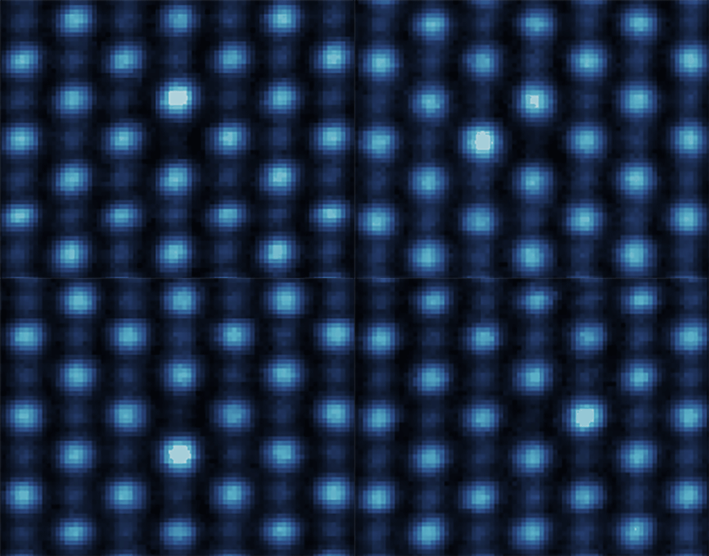
‘A new form of engineered artificial matter’: Atomic manipulation enters the mesoscale as 40,000 atoms repositioned in single crystal

Amazing stuff! "a new way to produce programmable matter in which ‘functionality is engineered from the atom up’." This could be huge!

"By creating 40,000 user-defined defects in a single crystal lattice, researchers have shown that atomic manipulation can be achieved on the mesoscopic scale – between the single-atom and bulk-material ranges. The work potentially offers a way to engineer materials with desired properties by fine-tuning the positions of individual atoms within their structures. ...

Now, a team from the US and Europe has scaled up the concept to a whole new level. Using the electron beam in a specially programmed scanning transmission electron microscope, the researchers introduced 40,000 defects into a chromium sulfur bromide lattice. The CrSBr semiconductor was selected as a model sample and, with their automated process, the researchers could subtly reposition individual chromium atoms in a predictable manner.
They describe the resulting material as ‘a new form of engineered artificial matter’, and note that it remains stable at room temperature outside of the microscope.

The defects were introduced within minutes across an area measuring 150nm × 100nm with a depth of 13nm. However, the team believes that the method is generalisable and could be scaled up to the macroscopic level. The researchers write that the technique offers a new way to produce programmable matter in which ‘functionality is engineered from the atom up’. ..."

"It’s been 37 years since scientists first demonstrated the ability to move single atoms, suggesting the possibility of designing materials atom by atom to customize their properties. Today there are several techniques that allow researchers to move individual atoms in order to give materials exotic quantum properties and improve our understanding of quantum behavior.

But existing techniques can only move atoms across the surface of materials in two dimensions. Most also require painstakingly slow processes and high-vacuum, ultracold lab conditions.

Now a team of researchers ... has created a way to precisely move tens of thousands of individual atoms within a material in minutes at room temperature. The approach uses a set of algorithms to carefully position an electron beam at specific locations of a material, then scan the beam to drive atomic motions. ..."

From the abstract:
"Controlling individual atoms using lasers, ion traps and scanning probe tips has transformed our understanding of matter and enabled breakthroughs in quantum science.
Extending this control into three-dimensional (3D) solids and across mesoscopic scales, however, remains a foundational challenge. Electron irradiation in electron microscopes is known to induce atomic displacements, and atomic manipulation has been proposed and demonstrated. Yet repeated and deterministic control has remained elusive.
Here we demonstrate deterministic atomic engineering in a 3D crystal, creating ordered arrangements of more than 40,000 user-defined defects within minutes across a 150 nm × 100 nm × 13 nm volume.
By steering individual Cr atoms in the magnetic semiconductor CrSBr into selected interstitial sites using an electron beam directed with sub-20-pm-scale accuracy, we create vacancy–interstitial complexes.
The resulting impurity array forms a mesoscale crystal embedded within the host lattice, a new form of engineered artificial matter that remains stable at room temperature and outside the microscope.
By tracking Cr atom displacements, we identify conditions under which the defect structures are predictable. Our calculations suggest that these defects form correlated impurity states with intra-defect optical transitions and inter-defect kinetic and Coulomb interactions.
This establishes a generalizable platform for atomic defect engineering at mesoscopic, and potentially macroscopic, scales, opening opportunities for scalable quantum technologies, including deterministic colour-centre placement, quantum simulation of many-body lattice models and atomic-scale manufacturing."

Scientists create 40,000 atomic defects in crystal to engineer programmable materials | Chemistry World

Researchers “reprogram” materials by quickly rearranging their atoms (original news release) "A new method for precisely moving columns of individual atoms within a material could give rise to exotic quantum properties."


Autonomous atomic engineering at scale by moving the electron beam between target locations. At each target location, the beam is positioned with picometre precision with chromium atoms then repositioned


“The results demonstrate the ability to deterministically move atoms repeatedly within a material’s 3D atomic lattice,” ... An animation shows how researchers controlled the movement of atoms.